ASE ICP Deep Silicon Etch System
Service Line: 02 Material Deposition and Etching
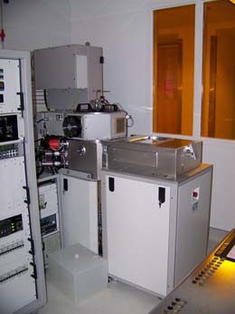
ASE ICP Deep Silicon Etch System
The Surface Technology System (STS) Advanced Silicon Etch (ASE®) ICP etch system achieves the high rate (microns/minute) anisotropic etching of silicon through a series of alternating passivation and etch steps: At the beginning of each cycle, a C4F8-based plasma is used to deposit a few conformal monolayers of a PTFE-like fluorocarbon polymer across all surfaces exposed to the plasma. The plasma gas is then switched to SF6 to create a plasma chemistry that etches silicon. Through the application of a DC bias to the plate, ions from the plasma bombard the surface of the wafer, removing the polymer. Increased ion energy in the vertical direction results in a much higher rate of removal of fluorocarbon from surfaces parallel to the wafer surface. Following selective polymer removal, the silicon surface at the base of the trench is exposed to reactive fluorine-based species that etch the unprotected silicon. The remaining fluorocarbon polymer protects the vertical walls of the trench from etching. By repeating the etch/passivation cycles and carefully controlling the etch time during each etch cycle, the degree of lateral etch is limited, allowing a trench to be etched vertically through the wafer. The ASE ICP etch system is capable of producing vertical etch depths of >0.5 mm, and aspect ratios approaching 20:1.
Manufacturer: STS
Model:
Contact:
Scott Williams
704-687-8126
scotwill@charlotte.edu
Tool Location:
Grigg Hall, Third Floor Room: CleanRoom Bay Number: 3